An govt visiting varied analysis divisions throughout the globe isn’t essentially new, however with a concentrate on social media driving named people at every firm to maintain their followers sitting on the sting of their seats signifies that we get much more insights into how these corporations function. The draw back of posting to social media is when sure pictures exposing unreleased info usually are not vetted by PR or authorized, and we get a glimpse into the subsequent era of know-how. That's what occurred immediately.
Day 1 with the @intel Israel group within the books. Nice views…unimaginable opp to see @GetThunderbolt innovation …a validation lab tour and time with the group…can’t wait to see what tomorrow brings! pic.twitter.com/GKOddA6TNi
— Gregory M Bryant (@gregorymbryant) August 1, 2021
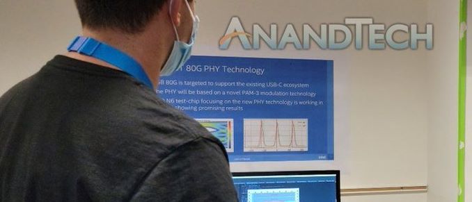
EVP and GM of Intel’s Consumer Computing Group, Gregory Bryant, is that this week spending a while at Intel’s Israel R&D services in his first abroad Intel journey in of 2021. An early submit on Sunday morning, showcasing Bryant’s journey to the fitness center to beat jetlag, was adopted by one other later within the day with Bryant being proven the workplaces and the analysis. The submit contained 4 images, however was quickly deleted and changed by a photograph with three (within the tweet above). The photograph eliminated showcases some new details about next-generation Thunderbolt know-how.
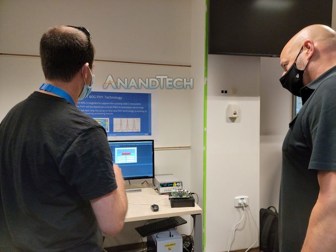
On this picture we are able to see a poster on the wall showcasing ‘80G PHY Know-how’, which signifies that Intel is engaged on a bodily layer (PHY) for 80 Gbps connections. Off the bat that is double the bandwidth of Thunderbolt 4, which runs at 40 Gbps.
The second line confirms that that is ‘USB 80G is focused to assist the present USB-C ecosystem’, which follows alongside that Intel is aiming to take care of the USB-C connector however double the efficient bandwidth.
The third line is definitely the place it will get technically fascinating. ‘The PHY will likely be based mostly on novel PAM-Three modulation know-how’. That is speaking about how the Zero and 1s are transmitted – historically we speak about NRZ encoding, which simply permits for a Zero or a 1 to be transmitted, or a single bit. The pure development is a scheme permitting two bits to be transferred, and that is referred to as PAM-4 (Pulse Amplitude Modulation), with the Four being the demarcation for what number of completely different variants two bits could possibly be seen (both as 00, 01, 10, or 11). PAM-4, on the similar frequency, thus has 2x the bandwidth of an NRZ connection.
So what on earth in PAM-3?
From Teledyne LeCroy on YouTube
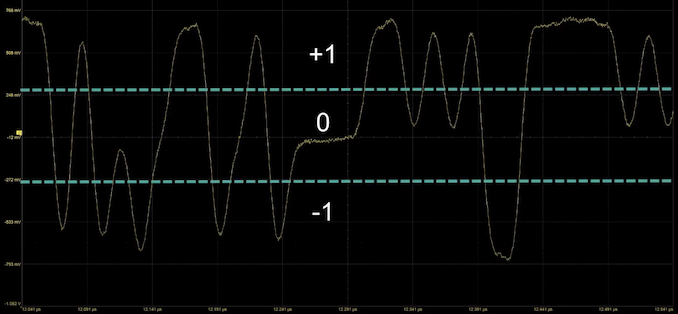
PAM-Three is a know-how the place the info line can carry both a -1, a 0, or a +1. What the system does is definitely mix two PAM-Three transmits right into a 3-bit information sign, reminiscent of 00Zero is an -1 adopted by a -1. This will get complicated, so here's a desk:
| PAM-Three Encoding | ||
| AnandTech | Transmit 1 |
Transmit 2 |
| 000 | -1 | -1 |
| 001 | -1 | 0 |
| 010 | -1 | 1 |
| 011 | 0 | -1 |
| 100 | 0 | 1 |
| 101 | 1 | -1 |
| 110 | 1 | 0 |
| 111 | 1 | 1 |
| Unused | 0 | 0 |
Once we evaluate NRZ to PAM-Three and PAM-4, we are able to see the speed of knowledge switch for PAM-Three is in the midst of NRZ and PAM-4. The explanation why PAM-Three is getting used on this case is to realize that greater bandwidth with out the additional limitations that PAM-Four requires to be enabled.
| NRZ vs PAM-Three vs PAM4 | |||
| AnandTech | Bits | Cycles | Bits Per Cycle |
| NRZ | 1 | 1 | 1 |
| PAM-3 | 3 | 2 | 1.5 |
| PAM-4 | 2 | 1 | 2 |
PAM-3 has related limitations to NRZ.
The ultimate line on this picture is ‘[something] N6 test-chip specializing in the brand new PHY know-how is working in [the lab and] displaying promising outcomes’. That first phrase I believed was TSMC, but it surely needs to be about the identical width because the ‘The’ on the road above. So it doesn’t appear like I’m proper there, however N6 is a TSMC node.
Intel’s purpose with Thunderbolt goes to be each driving bandwidth, energy, and utility, but in addition proper now it appears conserving it to the USB-C normal goes to be an important a part of conserving the know-how helpful for customers who can fall again on normal USB-C connections. Proper now Intel’s TB4 is a superset that features USB4, so we would see one other state of affairs the place TB5 is able to be a superset of USB5 as effectively, nonetheless plainly USB requirements are slower to roll out than TB requirements proper now.
Particular because of David Schor from WikiChip for the tipoff.
Posting Komentar
Posting Komentar