Previously week, TSMC ran its 2021 Expertise Symposium, masking its newest developments in course of node expertise designed to enhance the efficiency, prices, and capabilities for its prospects. On this occasion, TSMC mentioned its growing use of Excessive Extremely Violet (EUV) lithography for manufacturing, enabling it to scale right down to its 3nm course of node, properly past that of its rivals. TSMC additionally addressed the present points surrounding demand for semiconductors, together with asserting that it's constructing new amenities for superior packaging manufacturing. Becoming a member of CEO Dr. CC Wei as a part of the keynote presentation was AMD’s CEO Dr. Lisa Su, Qualcomm’s President (and shortly to be CEO) Cristiano Amon, and Ambiq’s Founder and CTO Scott Hanson.
As a part of the proceedings, TSMC supplied AnandTech a 30-minute interview with Dr. Kevin Zhang, SVP of Enterprise Growth, and Dr. Maria Marced, President of TSMC EU, as a chance to study extra about TSMC’s driving instructions in addition to cooperation with business companions. TSMC did request that we preserve the questioning solely on expertise issues and associated to the bulletins at its Expertise Symposium, relatively than focus on present international political matters.
 Kevin Zhang SVP Enterprise Growth |
 Maria Marced President, TSMC EU |
 Ian Cutress AnandTech |
Dr. Kevin Zhang has been TSMC’s Senior Vice President of Enterprise Growth for nearly a 12 months, having being promoted from the Design Expertise Workforce. Earlier to becoming a member of TSMC, Dr. Zhang spent 11 years at Intel as an Intel Fellow, turning into Vice President of the Expertise and Manufacturing Group in addition to Director of Circuit Expertise. Dr. Zhang has revealed over 80 papers in technical conferences and analysis journals, holds 55 patents in built-in circuit expertise, and holds a PhD in Electrical Engineering. Dr. Zhang would be the convention chair for ISSCC 2022.
Dr. Maria Marced is President of TSMC Europe, chargeable for driving technique and improvement of the corporate within the area, and has been within the place since 2007. Previous to this, Dr. Marced spent 4 years at NXP and 19 years at Intel in comparable top-position roles. Dr. Marced serves because the Chairwoman of the EMEA Management Council of the GSA (International Semiconductor Alliance), is on the board of CEVA, and holds a PhD in Telecommunications Engineering.
TSMC on The Main Edge
Ian Cutress: TSMC has acknowledged that it has had in-house EUV pellicle manufacturing since 2019, and TSMC is now vastly ramping up manufacturing of pellicles. How intensive is the use in manufacturing, and the way does it additional TSMC’s aggressive benefit versus different fabs?
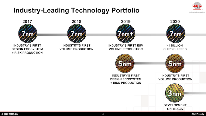
Kevin Zhang: We clearly have invested on this space in-house, and I believe it's a very distinctive expertise for us. We're capable of leverage it to deliver up our EUV mass manufacturing. If you happen to have a look at the way in which we ran our 7 nm, on the 6 nm, and now in 5 nm, all with the EUV, clearly now we have made super progress. So that is positively an space we expect now we have completed properly with our distinctive expertise benefit.
Maria Marced: One factor, as a result of I'm right here in Amsterdam, so we're comparatively near ASML - now we have had particular coaching by them. I can let you know, having this manufacturing in-house actually permits us to increase the lifetime of the masks. Usually in EUV, the masks will get soiled, and subsequently, with quick deadlines, this actually helps us rather a lot to enhance the productiveness of EUV and the masks.
IC: So by having it on web site means you’ve received much less journey for the masks, and it will get much less soiled as a consequence of much less journey?
MM: That’s appropriate.
IC: We usually affiliate complicated and specialty applied sciences with vanguard prospects. Provided that these prospects are sometimes within the low single digits, how does TSMC steadiness what packaging applied sciences to develop that prospects want, in comparison with creating and pathfinding new applied sciences?
KZ: On the main node, for instance, now we have been a frontrunner - a expertise chief. We need to proceed to drive development of silicon expertise, and we accomplice with our lead prospects to optimize our expertise. So that is positively an space we proceed to drive the longer term development. However with that being stated, I nonetheless suppose specialty expertise additionally performs a vital function in our general expertise providing to our prospects. A lot of our prospects can’t ship a single chip primarily based on to illustrate, 5 nm, with out possibly a 20 nm companion chip. If you happen to have a look at a cellphone for instance, there are a number of chips, and lots of companion chips. It's the similar factor with automotive - you've a complicated chip there, however you additionally want lots of microcontrollers primarily based on mature expertise.
So I believe now we have been doing a superb job in balancing our general expertise improvement effort. We now have invested in mature expertise considerably over the previous a long time. If you happen to have a look at our general expertise roadmap, we're offering probably the most superior specialty expertise providing at the moment within the market. I believe Maria possibly will add some shade from a Europe perspective.
MM: The one factor I'll add is that it is extremely vital for us to grasp the system complexity of our prospects. Additionally, particularly by having these applied sciences that full the invoice of supplies of the entire system, it helps us to higher perceive how the system architectures are evolving, and subsequently do a greater job for our prospects.
IC: So how a lot of that goes right down to what prospects are particularly demanding, versus researching new applied sciences that prospects do not know they want but?
KZ: We now have a separate crew, for instance, from a company standpoint. We now have a separate crew, a analysis crew issues past the following era. We actually look far out for that to discover various things. It additionally requires a lot of market enter, and buyer enter. to assist information a number of the exploratory work. So this can be a fairly dynamic course of, very interactive between us, inside us, and between us and the purchasers.
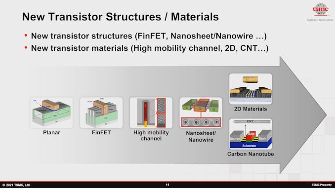
IC: TSMC has been very clear in saying that it's staying with FinFET, down to three nm, and transferring to Gate-All-Round at 2 nm. In contrast, the competitors is transferring to GAA at an earlier stage of improvement. Are you able to describe how TSMC is weighing each its want to be on the vanguard of those superior applied sciences, but additionally sustaining the identical FinFET for its manufacturing strains?
KZ: The explanation we selected FinFET expertise as a three nm is predicated on two issues.
One, now we have to determine a method to enhance the expertise into extra energy effectivity, extra efficiency, and the inner density. In the long run the client would not care whether or not it's FinFET, or Nanosheet. They need to have a look at it from their product standpoint - about what sort of energy, efficiency, and density profit it might deliver to the client. That is crucial factor in the long run. So we have a look at our FinFET expertise, and we have a look at our innovation functionality, we discover a very very highly effective knob, an modern knob, that permits us to increase the FinFET expertise down to three nm whereas additionally reaching substantial full node scaling advantages. In order that's cause primary.
Purpose quantity two can also be the schedule. We need to make certain, on the proper given time, we're capable of ship probably the most superior expertise. So predictability, from a complicated expertise improvement standpoint, may be very essential. Our prospects take scheduling very critically! So combining the 2, we decided to stick with the FinFET at 3nm. We imagine within the 2022-2023 timeframe, our three nm will deliver probably the most superior logic expertise to {the marketplace}.
IC: How do you steadiness pushing course of density versus design complexity, similar to 1D versus 2D steel routing? What are the present prospects on main nodes?
KZ: We have a look at all of the totally different metrics. On the finish of the day, we contemplate actually what it's at a product stage, at a system stage, and how much general scaling profit we are able to deliver the client. After I discuss in regards to the scaling advantages, I discuss with general energy/efficiency and the prices. This needs to be completed on the system stage, it is not merely on the chip stage.
Previously, two dimensional scaling dominated all the things, however now now we have to look extra at a system stage. For instance, you discover that we spend lots of effort and funding creating chip stage integration schemes: now we have 2D, 2.5D, and 3D going ahead. This all comes into play to principally present an entire system stage answer for the longer term. I believe you will notice increasingly functions primarily based on subtle superior chip stage integration expertise. Transistor improvement continues to be vital, make no mistake, and this can proceed to be very essential. Offering the client the most effective vitality environment friendly transistors continues to be very essential, however that is not going to be adequate.
We have a look at general scaling on the system stage. So a lot of co-optimization between expertise, totally different features of the expertise, and the product system stage design.
IC: As course of nodes shrink, resistance on steel layers is turning into extra problematic. With regards modern options, and unique supplies versus copper interconnects, is it only a case of extra analysis down that entrance? Or do we have to put extra effort into growing and routing larger steel layers?
KZ: I believe within the analysis session at our superior expertise introduction, we did cowl slightly bit in regards to the again finish work. For instance, we're persevering with to optimize the copper grain boundary to deliver a decrease resistance steel line to our general chip expertise and new expertise. Additionally, with dielectrics we proceed to seek out modern supplies to enhance the dielectric in parasitic capacitance. So, these issues are being actively researched.
The 3D integration also can deliver an alternate answer to this complete efficiency requirement within the back-end. You possibly can as an alternative route from A to B in a 2 dimensional area, or you possibly can route A to B vertically in three dimensions. In some instances, by going vertical, you possibly can cut back the general size of the RC wire, and cut back cross delay considerably. So all these issues must be checked out going ahead.
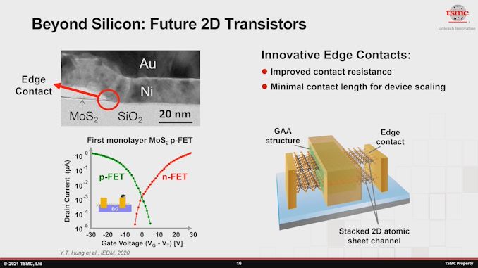
IC: So wanting into new applied sciences, the 2 most promising applied sciences as we transcend Gate-All-Round are 2D transistors and carbon nanotubes. TSMC lately launched a paper that received lots of press concerning new developments on 2D transistors. Are you able to touch upon what seems extra promising?
KZ: All these superior supplies for transistors have sure benefits. That is why we spend early R&D efforts to discover these, however these are nonetheless fairly far out. There are lots of issues that also have to be higher understood, particularly as it should take super effort to deliver these varieties of recent supplies, and new constructions, right into a large-scale manufacturing base. So there's nonetheless lots of work forward of us. However the good factor is we're not missing in new concepts. There are many new issues we're exploring, and so they all have a sure benefit. So we simply want to determine easy methods to combine all of them collectively to deliver out probably the most compelling general expertise answer to our future prospects' functions.
IC: Relating to the analysis in collaboration with ASML, they've spoken about future EUV developments similar to excessive NA (numerical aperture) optics. They preserve speaking to us about it! However as an extension of that, are you able to talk about what TSMC is essentially doing concerning post-EUV applied sciences?
KZ: We have a look at all totally different expertise choices. We talked slightly bit on the convention about materials improvements to deliver new supplies built-in on the silicon to permit us to attain higher conduction and a extra energy environment friendly transistor. These are vital areas by which now we have a analysis crew and an early R&D crew to develop and discover all totally different choices.
On lithography, clearly it continues to be a vital half in scaling the geometry. So we do have a crew additionally wanting into easy methods to maximize EUV, to print even tighter pitches going ahead. All these issues are being explored for the way forward for expertise choices.
Going Past Asia
IC: With reference to these most superior applied sciences, and vanguard capabilities, for Europe we have heard that the rivals of TSMC are investing of their European amenities. We have not essentially heard the identical from TSMC. Is there a specific cause for this? Or is there one thing that's to be introduced?
MM: Nicely, we wouldn’t rule out something. Nonetheless, at the moment, I shouldn't have any particulars to share with you!
IC: In your European prospects - just a few of them are form of on the vanguard? Most of them depend on the older course of applied sciences, specialty applied sciences - similar to the massive automotive business in Germany. We do not essentially see that there is lots of want to go vanguard from European enterprise. Are you able to remark?
MM: The principle segments in Europe are automotive, industrial, but additionally the place Europe is essential as properly is within the Web of Issues (IoT). The applied sciences which might be required by these segments are extra on the specialty facet, and extra on the superior, not solely mature, however superior applied sciences.
IC: We're clearly seeing lots of semiconductor demand for AI. A number of prospects need vanguard options, however there's additionally a lot of demand for edge merchandise on the extra mature nodes. Are you able to discuss to developments on how demand is shifting on the subject of AI, and maybe a point out of the EU on condition that China and North America will get the highlight?
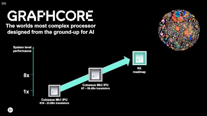
MM: Nicely, even within the UK, you've good AI firms! that certainly one of them is certainly one of our early adopter prospects in a number of initiatives (Ian: Graphcore already introduced working with TSMC at 3nm). But in addition in Israel, we see lots of exercise round AI. So in EMEA we see lots of curiosity in synthetic intelligence, and even the EU has some exercise leaning in the direction of what they name the European Processor Initiative (EPI), which revolves round the usage of synthetic intelligence.
So sure, we see lots of exercise. Truly, at the moment, I used to be very proud that in my presentation on the convention, I received an e mail from Matteo Vallejo from the College in Barcelona, which may be very a lot concerned in AI. So in fact, China and the US are all the time very superior in excessive efficiency computing, however we additionally see lots of curiosity in Europe, and lots of VC cash in AI.
IC: TSMC likes to advertise the place the income is coming from, and the proportion of income it receives from North America appears to be growing, on the expense of the proportion from Europe. Are there any headwinds or tailwinds about Europe that we must always take into consideration?
MM: The principle cause I believe is that as a result of Europe’s fundamental segments are automotive, industrial, and IoT. These segments are nonetheless utilizing mature superior applied sciences, and specialty applied sciences, and lots of these end-products have a decrease ASP, and this creates an enormous distinction when it comes to the share of revenues. How is that this transferring ahead? Quick, as a result of automotive, in addition to industrial, particularly as a part of business 4.zero and IoT, are as a result of AI choices are transferring quick in the direction of extra superior, extra vanguard expertise. So I actually anticipate that this proportion goes to alter considerably sooner or later.
IC: TSMC has three fundamental geographical areas - TSMC Asia, TSMC North America, and TSMC EMEA. How a lot are these unbiased group from one another - how a lot collaboration happens? Is it proper to be cut up, on condition that firms usually work worldwide or in a number of markets?
MM: Oh that is an attention-grabbing query! I actually imagine in firms being centralized, having labored at Intel for a few years (Maria was at Intel for 19 years), I actually imagine in firms being centralized and having one course coming from the management of the corporate. So we're not unbiased organizations in any respect! We're very depending on one another, and I can let you know I often spend most of my time touring to Taiwan - now video conferencing with Taiwan. However completely now we have one course, and we complement one another very properly. I believe Europe is bringing one thing totally different, which is targeted extra on and round specialties. That is the place we play the important thing function. We're actually one firm with one course.
Constructing and Increasing
IC: Pivoting to packaging, the CEO talked about that there are 5 fabs enabling SoIC and a brand new fab in Chunan with extra capability. Usually we measure manufacturing fabs in wafers monthly, so how ought to we contemplate the throughput of those new SoIC amenities?
KZ: I am unable to offer you a particular capability quantity, however all that I can say is that we're actually investing in our backend functionality and capacities. It is because we do see a pattern that increasingly prospects need to leverage our superior packaging choices, together with CoWoS, InFO, and going ahead, SoIC with 3D integration. In order that's why we're investing not solely within the R&D facet, however we're additionally investing within the capability facet to arrange for future development.
With 3D packaging capability metrics, it will depend on what sort of configuration you do. Generally you would probably do a really superior chiplet built-in with extra mature nodes, and minus one or minus two nodes, so that you simply in all probability must compute the full quantity in another way. All of it will depend on the precise product configuration. Possibly sooner or later, we'll have to determine a method to higher measure the amount and report the numbers. For the definition quantity, once you come to 3D integration, it might be that we rely the variety of last built-in components.
IC: TSMC at the moment has 4 packaging amenities, and this fifth one (known as AP6) is being inbuilt Chunan. AP6 would have over 50% of the packaging capability of TSMC globally. Are there any optimistic or damaging implications for having a big portion of all TSMC’s packaging in a single space?
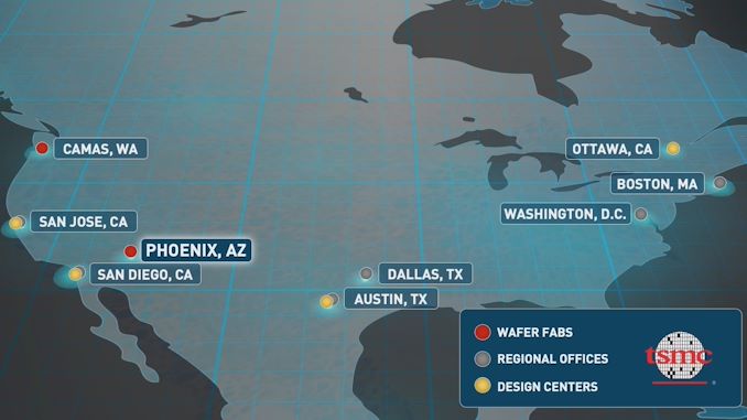
KZ: We do lots of balancing - there's a bonus for us by constructing a bigger scale manufacturing facility. I believe you in all probability already know that we construct Gigafabs at the moment with massive scales. I believe that that is a key financial profit that we are able to deliver to our prospects, enabling decrease prices that can even be handed on to the client. However we do must have issues on easy methods to unfold that to totally different areas. We're doing that, ensuring we preserve a sure steadiness. In an analogous mild, we're constructing a manufacturing unit in Arizona fairly distant from Taiwan!
IC: Talking about packaging and OSAT bottlenecks. When talking with our viewers, quite a lot of them appear to suppose it's wafer throughput, and a few of them imagine it comes right down to packaging throughput. I do not essentially need to ask you about which one is probably the most bottlenecked however I do need to ask about how TSMC is bettering throughput of buyer orders. We’ve spoken about TSMC increasing its packaging, however is there something TSMC can do right here?
KZ: I believe on the technical half, your readers need to view it as both the wafer expertise is the bottleneck, or the packaging applied sciences are the bottleneck. Truly the way in which I have a look at it's how we're discovering the optimum answer to deliver all of the items collectively at a system stage to offer the most effective consequence. If you happen to look again at semiconductor expertise, it began with two dimensional issues, and Moore's legislation is in regards to the transistor density, scaling, and economics. However now as we're transferring ahead, I see the entire business trending as we transfer in the direction of a better stage of integration. In technical conferences, similar to ISSCC, you see folks not solely discuss transistor stage design, however in addition they discuss system stage efficiency, and easy methods to deliver all the features and all of the items collectively. Sooner or later, I believe that this pattern will proceed, so it is actually about working together with your prospects for his or her given product utility, given their distinctive system stage necessities, and the way you deliver all the items collectively in an optimum style. That is how I have a look at it sooner or later.
MM: Our key factor is that we collaborate to innovate. Collaborating with our prospects is our greatest method to actually innovate, permitting their improvements and on the similar time boosting our personal improvements.
IC: DTCO (Design Expertise Co-Optimization) is an integral a part of making most out of vanguard applied sciences. Is DTCO getting extra complicated, or as TSMC and its prospects perceive the method behind reaching good DTCO, is it accelerating? Are you able to discuss that?
KZ: I believe our prospects have benefited drastically from design expertise co-optimization over the past couple of generations. Going ahead, there shall be extra DTCO to do, and we discover our prospects are extra keen and keen to collaborate with us with a purpose to harvest intrinsic expertise advantages. I believe this pattern will proceed and I believe the trouble even then shall be stronger going ahead. As they have to be extra intertwined between expertise and the design, you would name it tougher? I believe it should turn out to be extra delicate, and we have to work nearer with our prospects to essentially optimize issues collectively. Now you even have superior packaging coming in, so how a system can partition its expertise may fluctuate. When you have a chiplet, the way you architect it at a system stage from the get-go, you must take into consideration easy methods to architect your system in the fitting method by leveraging totally different items of silicon expertise and totally different integration schemes.
Many due to Kevin, Maria, and TSMC's Comms groups for his or her time.
Additionally due to Gavin Bonshor for transcription.
Posting Komentar
Posting Komentar