In immediately’s Intel Accelerated occasion, the corporate is driving a stake into the bottom concerning the place it desires to be by 2025. CEO Pat Gelsinger earlier this 12 months acknowledged that Intel can be returning to product management in 2025, however hasn’t but defined how that is coming about – that's till immediately, the place Intel has disclosed its roadmap for its subsequent 5 generations of course of node expertise resulting in 2025. Intel believes it may comply with an aggressive technique to match and move its foundry rivals, whereas on the identical time creating new packaging choices and beginning a foundry enterprise for exterior clients. On prime of all this, Intel has renamed its course of nodes.
The Brief Reply:
When you solely take one factor away from this text, I'll put it right here entrance and heart. Here's what we're seeing for Intel's roadmaps, based mostly on their disclosures immediately.
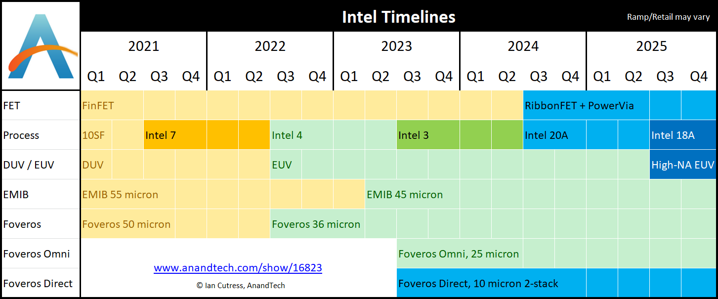
As at all times, there's a distinction between when a expertise ramps for manufacturing and involves retail; Intel spoke about some applied sciences as 'being prepared', whereas others have been 'ramping', so this timeline is solely these dates as talked about. As you may think, every course of node is more likely to exist for a number of years, this graph is solely showcasing the main expertise from Intel at any given time.
If you'd like the small print on this graph, then learn on.
Intel's Defines a Robust Future: Is TSMC at Danger?
Earlier this 12 months, CEO Pat Gelsinger introduced Intel’s new IDM 2.zero technique, consisting of three parts:
- Construct (7nm)
- Broaden (TSMC)
- Productize (Intel Foundry Providers)
The aim right here is to proceed to work on Intel’s course of node expertise growth, going past the present 10nm designs in manufacturing immediately, however concurrently utilizing different foundry providers from companions (or opponents) to regain/retain Intel’s place in its processors that drive a variety of the corporate income. The third factor is IFS, Intel’s Foundry Providers, the place Intel is committing in a giant approach to opening up its manufacturing amenities to exterior semiconductor enterprise.
Underpinning (1) and (3) is how Intel executes by itself course of node growth. Whereas in Intel’s latest Q3 2021 earnings name CEO Gelsinger confirmed that Intel is now producing extra 10nm wafers in a day than 14nm wafers, marking a shift in confidence between the 2 designs, it's no secret that Intel has had problem in transitioning from its 14nm course of to its 10nm course of. On June 29th this 12 months, Intel additionally acknowledged that its subsequent technology 10nm product requires further validation time to streamline deployment on enterprise techniques for 2022. Notice that on the identical time, TSMC has surpassed Intel by delivery at capability with its equal designs (referred to as 7nm) and its vanguard (5nm) designs that surpass Intel’s efficiency.
As with the earlier announcement in March, Intel is reaffirming that it intends to return to management efficiency in semiconductors in 2025. This may allow each the corporate to compete higher because it builds its personal merchandise (1) but in addition provide a wider portfolio of efficiency and applied sciences for its future IFS clients (3). To do that, it's realigning the roadmap for its future course of node applied sciences to be extra aggressive with enhancements, but on the identical time extra modular with its expertise to allow sooner transitions.
Main up this plan is Dr. Ann B Kelleher, who was named SVP and GM of the Know-how Growth division at Intel final 12 months. This division is the place all of the analysis and growth of Intel’s future course of node applied sciences and enhancements comes from – it was a part of Intel’s System Structure Group, nevertheless it was break up in July 2020 to re-establish a spotlight purely on Know-how Growth. Dr. Kelleher’s background includes course of analysis in academia, adopted by 26 years at Intel as a course of engineer, transferring as much as managing Fab 24 in Eire, Fab 12 in Arizona, Fab 11X in Rio Rancho, earlier than touchdown in HQ in Oregon because the GM of Manufacturing and Operations.
Her expertise protecting each fab-scale manufacturing and course of node analysis goes to be vital for Intel’s future plans. In discussing with Kelleher forward of immediately’s bulletins, she acknowledged that she has applied basic modifications relating to provider method, ecosystem learnings, organizational modifications, modular design methods, contingency plans, and realigning the Know-how Growth Workforce right into a extra streamlined outfit able to execute. These embody key personnel reminiscent of Sanjay Natarajan as SVP and GM of Logic Growth (considered one of Intel’s latest rehires) and Babak Sabi as CVP and GM of Meeting/Take a look at Growth
Intel is immediately defining ‘expertise management by 2025’ as outlined by the metric of efficiency per watt. We requested Intel is a pre-briefing what which means for peak efficiency, which is commonly a metric we care about for finish product design, and the reply was that "peak efficiency stays a key a part of Intel’s strategic growth".
Intel Renames The Nodes: ‘Mine is Smaller’
The issue with merely posting Intel’s roadmap right here is that the information is two-fold. Not solely is Intel disclosing the state of its expertise for the subsequent a number of years, however the names of the expertise are altering to higher align with frequent business norms.
It's no secret that having "Intel 10nm" being equal to "TSMC 7nm", though the numbers truly don't have anything to do with the bodily implementation, has floor at Intel for some time. Lots of the business, for no matter motive, hasn’t discovered that these numbers aren’t truly a bodily measurement. They was, however after we moved from 2D planar transistors to 3D FinFET transistors, the numbers grew to become nothing greater than a advertising device. Regardless of this, each time there’s an article concerning the expertise, individuals get confused. We’ve been speaking about it for half a decade, however the confusion nonetheless stays.
To that finish, Intel is renaming its future course of nodes. Right here’s the roadmap picture, however I’ll be breaking it down piece by piece.
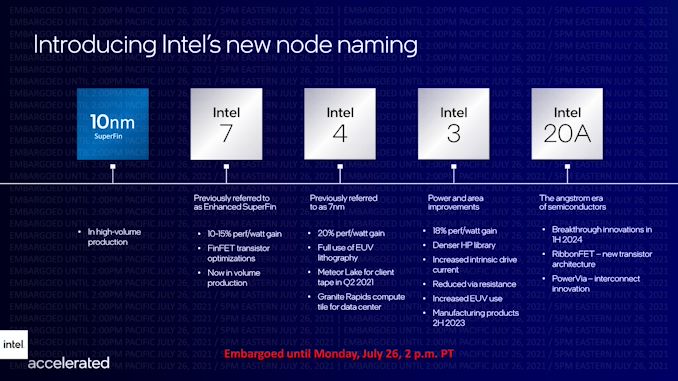
2020, Intel 10nm SuperFin (10SF): Present technology expertise in use with Tiger Lake and Intel’s Xe-LP discrete graphics options (SG1, DG1). The title stays the identical.
2021 H2, Intel 7: Beforehand generally known as 10nm Enhanced Tremendous Fin or 10ESF. Alder Lake and Sapphire Rapids will now be generally known as Intel 7nm merchandise, showcasing a 10-15% efficiency per watt acquire over 10SF because of transistor optimizations. Alder Lake is presently in quantity manufacturing. Intel’s Xe-HP will now be generally known as an Intel 7 product.
2022 H2, Intel 4: Beforehand generally known as Intel 7nm. Intel earlier this 12 months acknowledged that its Meteor Lake processor will use a compute tile based mostly on this course of node expertise, and the silicon is now again within the lab being examined. Intel expects a 20% efficiency per watt acquire over the earlier technology, and the expertise makes use of extra EUV, largely within the BEOL. Intel’s subsequent Xeon Scalable product, Granite Rapids, can even use a compute tile based mostly on Intel 4.
2023 H2, Intel 3: Beforehand generally known as Intel 7+. Elevated use of EUV and new excessive density libraries. That is the place Intel’s technique turns into extra modular – Intel Three will share some options of Intel 4, however sufficient will likely be new sufficient to explain this a brand new full node, particularly new excessive efficiency libraries. Nonetheless, a quick comply with on is anticipated. One other step up in EUV use, Intel expects a producing ramp within the second half of 2023 with an 18% efficiency per watt acquire over Intel 4.
2024, Intel 20A: Beforehand generally known as Intel 5nm. Transferring to double digit naming, with the A standing for Ångström, or 10A is the same as 1nm. Few particulars, however that is the place Intel will transfer from FinFETs to its model of Gate-All-Round (GAA) transistors referred to as RibbonFETs. Additionally Intel will debut a brand new PowerVia expertise, described under.
2025, Intel 18A: Not listed on the diagram above, however Intel is anticipating to have an 18A course of in 2025. 18A will likely be utilizing ASML’s newest EUV machines, generally known as Excessive-NA machines, that are able to extra correct photolithography. Intel has acknowledged to us that it's ASML’s lead companion relating to Excessive-NA, and is about to obtain the primary manufacturing mannequin of a Excessive-NA machine. ASML lately introduced Excessive-NA was being delayed- when requested if this was a difficulty, Intel stated no, because the timelines for Excessive-NA and 18A are the place Intel expects to intersect and have unquestioned management.
Intel has confirmed to us that Intel Three and Intel 20A will likely be provided to foundry clients (however hasn’t acknowledged if Intel Four or Intel 7 will likely be).
To convey this altogether in a single desk, with recognized merchandise, we now have the next:
| Intel's Course of Node Know-how | ||||
| Previous Identify | New Identify | Roadmap | Merchandise | Options |
| 10SF | 10SF | At the moment | Tiger Lake SG1 DG1 Xe-HPC Base Tile Agilex-F/I FPGA | SuperMIM Skinny Movie Barrier Quantity 10nm On sale immediately |
| 10ESF | Intel 7 | 2021 H2 merchandise | Alder Lake (21) Raptor Lake (22)? Sapphire Rapids (22) Xe-HP Xe-HPC IO Tile | 10-15% PPW Upgraded FinFET ADL in Ramp immediately |
| 7nm | Intel 4 | 2022 H2 ramp 2023 H1 merchandise | Meteor Compute Tile Granite Compute Tile | 20% PPW vs 7 Extra EUV Silicon in Lab |
| 7+ | Intel 3 | 2023 H2 merchandise | - | 18% PPW vs 4 Space Financial savings Extra EUV New Perf Libraries Sooner Observe On |
| 5nm | Intel 20A | 2024 | - | RibbonFET PowerVia |
| 5+ | Intel 18A | 2025 | Unquestioned Management | 2nd Gen Ribbon Excessive NA EUV |
One of many points right here is the distinction between a course of node being prepared, ramping manufacturing for product launches, and truly being made obtainable. For instance, Alder Lake (now on Intel 7nm) is because of come out this 12 months, however Sapphire Rapids goes to be extra of a 2022 product. Equally, there are experiences of Raptor Lake on Intel 7 popping out in 2022 to exchange Alder Lake with the tiled Meteor Lake on Intel Four in 2023. Whereas Intel is completely happy to debate course of node growth time frames, product timeframes should not as open (as little question clients would get annoyed if the time acknowledged is missed).
Why The Nodes Had been Renamed
In order acknowledged earlier than, one factor of renaming the nodes is because of matching parity with different foundry choices. Each TSMC and Samsung, opponents to Intel, have been utilizing smaller numbers to match related density processes. With Intel now renaming itself, it will get extra in-line with the business. That being stated, maybe sneakily, Intel’s 4nm is likely to be on par with TSMC’s 5nm, reversing the tables. By 3nm we anticipate there to be a superb parity level, nevertheless that may rely on Intel matching TSMC’s launch schedule.
Fairly than throw course of node names in every single place, it's typical to confer with peak quoted transistor densities as a substitute. Right here is the desk we revealed in our latest IBM 2nm information submit, however with an up to date shift on Intel’s naming.
| 2021 Peak Quoted Transistor Densities (MTr/mm2) | ||||
| AnandTech Course of Identify | IBM | TSMC | Intel | Samsung |
| 22nm | 16.50 | |||
| 16nm/14nm | 28.88 | 44.67 | 33.32 | |
| 10nm | 52.51 | 100.76 | 51.82 | |
| 7nm | 91.20 | 100.76 | 95.08 | |
| 5/4nm | 171.30 | ~200* | 126.89 | |
| 3nm | 292.21* | |||
| 2nm / 20A | 333.33 | |||
| Knowledge from Wikichip, Completely different Fabs might have totally different counting methodologies * Estimated Logic Density | ||||
Precisely the place Intel’s new 4nm and under will find yourself is but to be disclosed, as numbers with stars alongside are based mostly on estimates by the respective corporations.
It has been anticipated for some time that Intel can be realigning its course of node naming. Behind closed doorways, I personally have been lobbying for it for some time, and I do know that a couple of different journalists and analysts have been suggesting it to Intel as properly. Some responses we acquired have been associated to apathy – one govt instructed me that "our clients that care about this truly know the distinction", which is true for certain, however what we’re speaking about right here is extra about notion within the wider ecosystem for fans and monetary analysts who won't be in control. It is kind of a branding train, and I additionally instructed Intel that they're going to need to anticipate a blended response – some voices would possibly interpret the transfer as Intel making an attempt to tug one over in the marketplace, for instance. However they’re going to need to stay with it, as these are the brand new names.
In the meantime, regardless of Intel’s struggles with 10nm, it's nonetheless a course of node in manufacturing and in quantity manufacturing, in use for each client and enterprise units, and it is coming to desktops very quickly. Though it has some stiff competitors from different gamers, it's nonetheless an providing out there, and for those who wish to evaluate course of node densities utilizing these names, it ought to have a moniker to keep away from confusion. I'm applauding that Intel is doing it sooner slightly than later.
One key level to notice is that the brand new Intel 7 node, which was previously the 10ESF node, shouldn't be essentially a "full" node replace as we usually perceive it. This node is derived as an replace from 10SF, and because the diagram above states, can have ‘transistor optimizations’. Transferring from 10nm to 10SF, that meant SuperMIM and new thin-film designs giving an additional 1 GHz+, nevertheless the precise particulars from 10SF to the brand new Intel 7 is unclear at this level. Intel has nevertheless acknowledged that transferring from Intel 7 to Intel Four will likely be an everyday full node leap, with Intel Three utilizing modular elements of Intel Four with new high-performance libraries and silicon enhancements for an additional leap in efficiency.
We requested Intel if these course of nodes can have further optimization factors, and have been instructed that they'll – whether or not any of them will likely be explicitly productized will rely on the options. Particular person optimizations might account for an extra 5-10% efficiency per watt, and we have been instructed that even 10SF (which retains its title) has had a number of further optimization factors that haven’t essentially been publicized. So whether or not these updates get marketed as 7+ or 7SF or 4HP shouldn't be recognized, however as with all manufacturing course of as updates happen to assist enhance efficiency/energy/yield, they get utilized assuming the design adheres to the identical guidelines.
"Is not Intel Simply Attempting To Pull The Wool Over Our Eyes?"
No.
The issue right here is that there isn't any constant node naming between foundries. Intel has been saving any quantity change for main advances in its node manufacturing expertise, as a substitute utilizing +/++ to indicate enhancements. If we evaluate this to TSMC and Samsung, each of whom have been completely happy to present half-node jumps new numbers fully.
For instance, Samsung's 7LPP is a serious node, nevertheless 6LPP, 5LPE and 4LPE are all iterative efforts on the identical design (arguably additionally iterative of 8LPP), with 3GAE being the subsequent main leap. Evaluate this to Intel, who was planning 10nm to 7nm to 5nm as main course of node jumps – so whereas Samsung had one leap deliberate and Four sub-variants (or extra), Intel had two main jumps. Equally, TSMC's 10nm was a half-node leap over 16nm, whereas 16nm to 7nm was the total node – Intel made 14 to 10 to 7 as full nodes.
Intel caught to its weapons a protracted whereas, and delays to 10nm successfully harm it in a multiplicative vogue. For instance, if Intel had labeled 14+ as 13nm, and 14++ as 12nm, maybe it would not be so unhealthy. I imply, sure Intel ought to anticipate some harm for 10nm being late, however when different foundries have been showcasing smaller steps as full quantity jumps, it grew to become a advertising and media nightmare. 14++++ grew to become an business joke, and matched with how each time after they talked about future course of nodes they needed to cite the equal TSMC of Samsung course of, it acquired a bit an excessive amount of. It needed to be defined each time, as new individuals come into the business.
I've lobbied Intel to regulate its naming for some time, and I do know different friends have as properly. Once we confer with Intel 7 any further, we are able to draw equivalents to TSMC 7nm (even when TSMC is delivery 5nm in quantity) with out having to extensively clarify variations in a easy title. This is not Intel pulling the wool over your eyes, or making an attempt to cover a foul state of affairs. That is Intel catching as much as the remainder of the business in how these processes are named. So as to add to this, it is a good factor that Intel is simply renaming future nodes that have not reached the market but.
It is a multi-page article!
Click on the dropdown under for extra pages, together with
- This Web page, New Node Names
- A Sidebar on Intel EUV and turning into ASML Lead Associate
- New for 2024: RibbonFETs and PowerVias
- Subsequent Gen EMIB and Foveros Packaging
- Prospects Prospects Prospects
Posting Komentar
Posting Komentar